Next: Implementing Digital Delay Lines Up: Delay Lines Previous: Delay Lines
 (see the -Transform).
![$x[n], n = 0, 1, 2, \ldots$](img74.png) . For a delay line length of
. For a delay line length of  samples, the output is given by the relation
![$\displaystyle y[n] = x[n - M], \hspace{0.2in} n = 0, 1, 2, \ldots,
$](img75.png)
![$x[n] \ensuremath{\stackrel{\Delta}{=}}0$](img17.png) for
for  .
.
 .
.
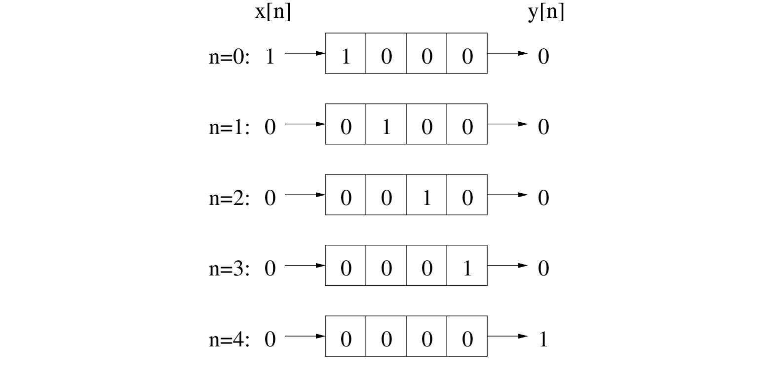
 and a discrete-time unit impulse input signal defined as
![$\displaystyle x[n] = \left\{ \begin{array}{ll} 1, & n = 0 \\
0, & n \neq 0. \end{array} \right.
$](img77.png)
 , the signal value in the last (right-most) memory location is output from the delay line, the remaining stored values are propagated to adjacent memory locations (to the right), and a new input sample is written to the first (left-most) memory location.
 will appear at the delay line output at time step
  . For this particular example, all subsequent inputs and outputs to the delay line are zeroes. In this way, the finite length impulse response of the length digital delay line is given by
 .
.
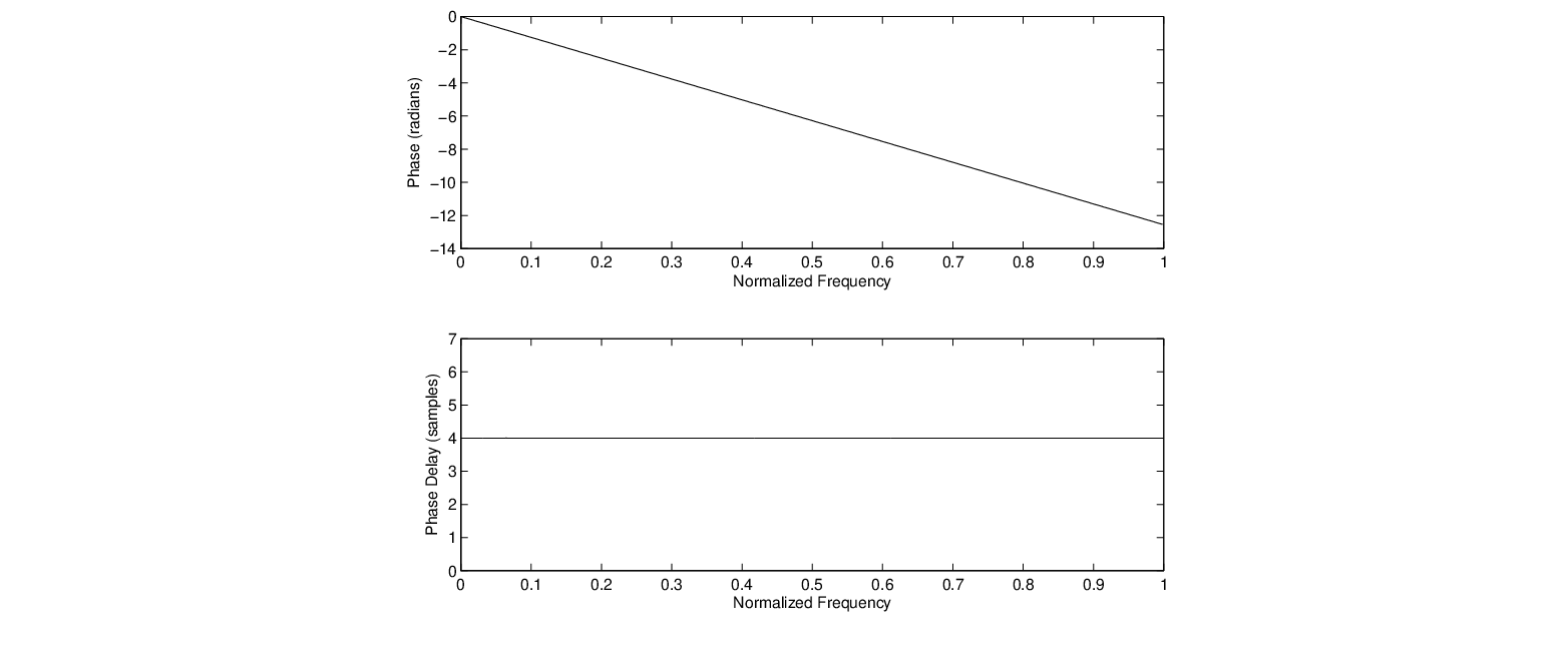
delay line system is shown in Fig. 9, plotted both in radians (top) and as phase delay (negative phase divided by frequency) in samples (bottom), from which its linear phase response is clear.

| ©2004-2024 McGill University. All Rights Reserved. Maintained by Gary P. Scavone. |
![\begin{figure}\begin{center}
\begin{picture}(3.5,0.5)
\put(0.26,0){\epsfig{fil...
...,0.16){$x[n]$}
\put (3.5,0.16){$y[n]$}
\end{picture} \end{center}
\end{figure}](img73.png)